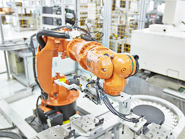

With many years of mold design and manufacturing experiences, Keboda's design and development capabilities for automatic continuous deep drawing stamping die are ahead of domestic counterparts.
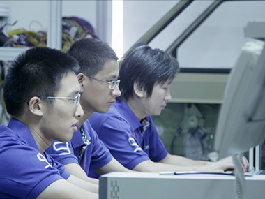
With an experienced and capable process development team, Keboda has been committed to providing first-class process solutions for many years, providing advanced production line equipment, test equipment, development equipment, tooling and fixtures.
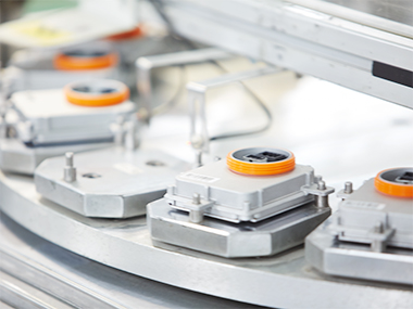
The technology in the field of the automotive parts process has formed a complete process chain from SMT, DIP to ASSEMBLY. In the field of SMT, Keboda has mastered and introduced the world's leading laser marking and vacuum reflow technology. The smallest chip size is 0402/0201, the maximum is 100*90*21mm, the chip spacing is 0.3mm minimum, the PCBA design can achieve 24 layers; and the chip technology of aluminum substrate has been mastered and introduced. The DIP section has mastered and introduced wave soldering and selective wave soldering techniques. In the latter stage of the ASSEMBLY field, advanced online ICT, online sub-plate, connector crimping, automatic point coating, potting, automatic welding, automatic locking screw, coating technology and other processes were introduced.
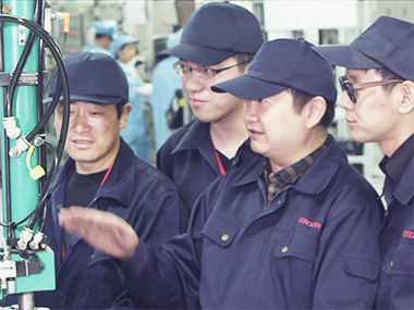
In addition to focusing on the automotive body electronics and powertrain processes, Keboda also researched many advanced technologies, including automotive new energy products.